Dr. Kai Xiao
Functional Nanomaterials Synthesis, Properties, and Devices
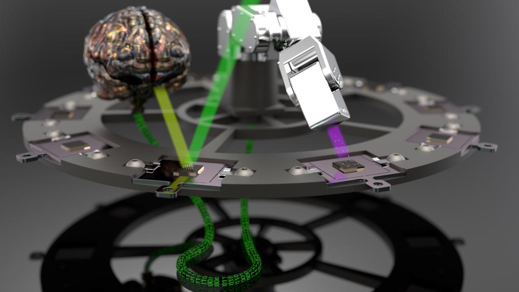
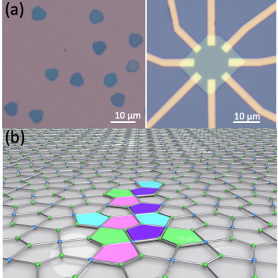
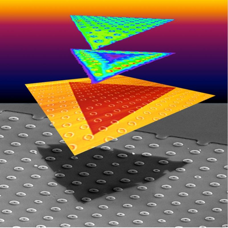
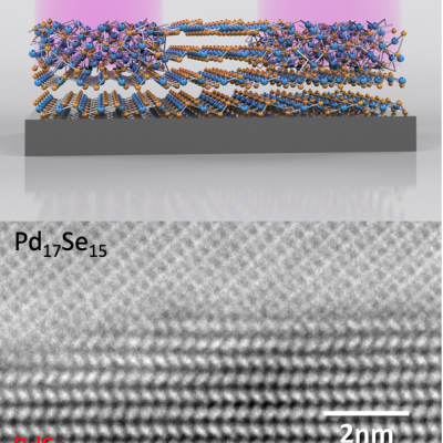
Dr. Xiao is a distinguished staff scientist in the Functional Hybrid Nanomaterials Group at Center for Nanophase Materials Sciences, ORNL and a joint faculty at the Bredesen Center and Department of Computer Science and Electrical Engineering, University of Tennessee at Knoxville. He obtained his Ph.D. degree in Physic Chemistry in 2004 from Institute of Chemistry, Chinese Academy of Sciences. Then he worked as a postdoc associate at CNMS and became a staff scientist in 2008. Currently, his research focuses on developing and applying advanced synthesis/processing (CVD, PLD, laser processing, etc.) coupled with time-resolved in situ diagnostics (XRD, neutron, optical spectroscopies, and TEM/STEM) to understand and control functional nano materials and devices for microelectronics and quantum information science. He also leads on growth mechanisms and controlled synthesis of 2D quantum materials and heterostructures, including autonomous synthesis with automation, AI/ML, and in situ diagnostics. He has published about 210 papers, several patents, and 7 book chapters.
Professional and Synergistic Activities:
Focus issue, Symposium and Workshop Organizer,
- The Focus Section: Heterogeneity in Beyond Graphene 2D Materials in JMR, Vol 35, issue 11, 2020. (Co-editor with Zakaria Balushi and Sefaattin Tongay)
- Emerging 2D Non-Graphene Materials in XXVII International Materials Research Congress (IMRC2018). Co-organized with Deji Akinwande (University of Texas at Austin) and Talat Rahman (UCF)
- Synthesis and Collective Phenomena in 2D and Layered materials workshop in 2017 Joint Nanoscience and Neutron Scattering User Meeting, 2017. (Co-organized with David Mandrus and Travis Williams)
Editorial and Conference Board, Review and Service:
- Steering committee member of 17th International Conference on Laser Ablation (COLA), 2024.
- Co-chair of the 70th AVS 2D Materials Technical Group (2DMTG) Executive Council (EC), Tampa, FL, 2024
- Sectary of the 69th AVS 2D Materials Technical Group (2DMTG) Executive Council (EC), 2023.
- The committee member of the ‘2D Materials Focus Topic’ Program Committee for the AVS 65th International Symposium & Exhibition (2018)
- International Advisory Committee of the International Conference on Computational Mathematics in Nanoelectronics and Astrophysics (CMNA 2018), India
- International Advisory Committee Member for the Centre for Advanced Electronics at Indian Institute of Technology (IIT) Indore (2020)
Proposal Reviewer:
NSF Reviewer Panels on Organic Electronics, Materials Engineering and Processing (MEP) Program and Photonic Devices, Electronics, Photonics and Magnetic Devices (EPMD) program; DOE-BES; Moore Foundation; The European Research Council (ERC); The Netherlands Dutch Research Council (NWO); ORNL seeds and LDRD; User proposal reviewer for the Molecular Foundry at Laurence Berkeley National laboratory and Stanford Synchrotron Radiation Lightsource (SSRL); the Czech Science Foundation and Israel Science Foundation.
Journal Reviewer:
Nature, Nature Nano; Nature Materials; Nature Chem; Nature Comm.; Light: Science & Applications; NPG Asia Materials; Scientific Report; J. Am. Chem. Soc.; Nano Letters, J. Phys. Chem. B; Chem. Mater.; ACS Nano; Langmuir; Angew. Chem. Int. Ed.; Adv. Mater.; Adv. Func. Mater.; Adv. Energy Mater.; Small; ChemSusChem; PCCP; Chem. Eur. J; Appl. Phys. Lett.; Phys Rev Lett; Phys Rev B; Phys Rev Mater; Nanoscale; J. Mater. Chem.; Polymer Chemistry; Polymer Reviews; J. Appl. Polymer Sci.; 2D Materials; Materials Today
Honors and Awards:
- The Nano Research Young Innovators (NR45) Awards in two-dimensional materials, 2021
- UT-Battelle Outstanding Scholarly Output Award, 2020
- CNMS Distinguished Scientific Paper Award, 2017
- CNMS Distinguished Scientific Paper Award, 2014
Research Projects:
- DOE-BES Scientific User Facilities Division, Center for Nanophase Materials Sciences
- PI, DOE-BES Materials Science and Engineering Division, 2021-present, “Growth Mechanisms and Controlled Synthesis of Nanomaterials.”
- Co-PI, DOE-BES Materials Science and Engineering Division, 2015-2021, “Growth Mechanisms and Controlled Synthesis of Nanomaterials.”
- Co-PI, DOE NSRC-QIS, 2018-2021, “Thin Film Platform for Rapid Prototyping of Novel Materials with Entangled States for QIS”
- PI, ORNL-LDRD, 2013-2015, “Synthesis and Characterization of Novel Two-Dimensional Mesoscale Organic Nanomembranes”
- Co-PI, DOE-EERE, “Novel photon management for thin-film photovoltaics”
- Co-PI, ORNL-LDRD, “Rational design of deuterated conjugated polymers with controlled spin-polarized electron transport”

