Research Interests

My current research foci are: (1) synthesis of functional 2D materials for electronics and quantum information science; (2) understanding the fundamental growth process and mechanism of functional nanomaterials; (3)  quantum transport, FET, photodetector and other devices of 2D materials (4) solution-processing organic and hybrid perovskites electronics and solar cells.

Research Capabilities

See the Signature Capabilities in our group.

Overview of different types of heterogeneities at multiple length scales in 2D materials and their functionalities and applications
Raman, PL and SHG reveal how strain impacts growth and optical properties of a monolayer 2D crystal of WS2 grown on patterned donuts on substrates.

Understanding and controlling the heterogeneity in 2D quantum materials through controlled synthesis and processing

Two dimensional (2D) materials have great promise for applications in optoelectronics, quantum information science and energy conversion due to their remarkable properties imbued by their physical characteristics. Although heterogeneities in their intrinsic structure are the major challenge limiting their synthesis and predictable properties, they also provide a pathway to controllably tune the properties and broaden the potential of 2D materials. Heterogeneities that can be tailored, including defects, dopants, strain, edges, and stackings have offered new transformative opportunities in heterogeneous 2D materials through the introduction of novel properties for technological applications. We are working on engineering the specific types of heterogeneities through novel synthesis and processing methods for the potential impact and applications enabled by their intriguing properties. We are interested  in developing a strategy that involves in situ optical diagnostics to control synthesis and processing, atomistic characterization methods to identify heterogeneities, device measurements to measure the impact on mesoscale properties, and predictive/responsive theory and computational modeling. Our strategy enables a comprehensive understanding of the roles of heterogeneities in delivering novel mesoscopic properties and functionalities that could lead to exciting applications. 

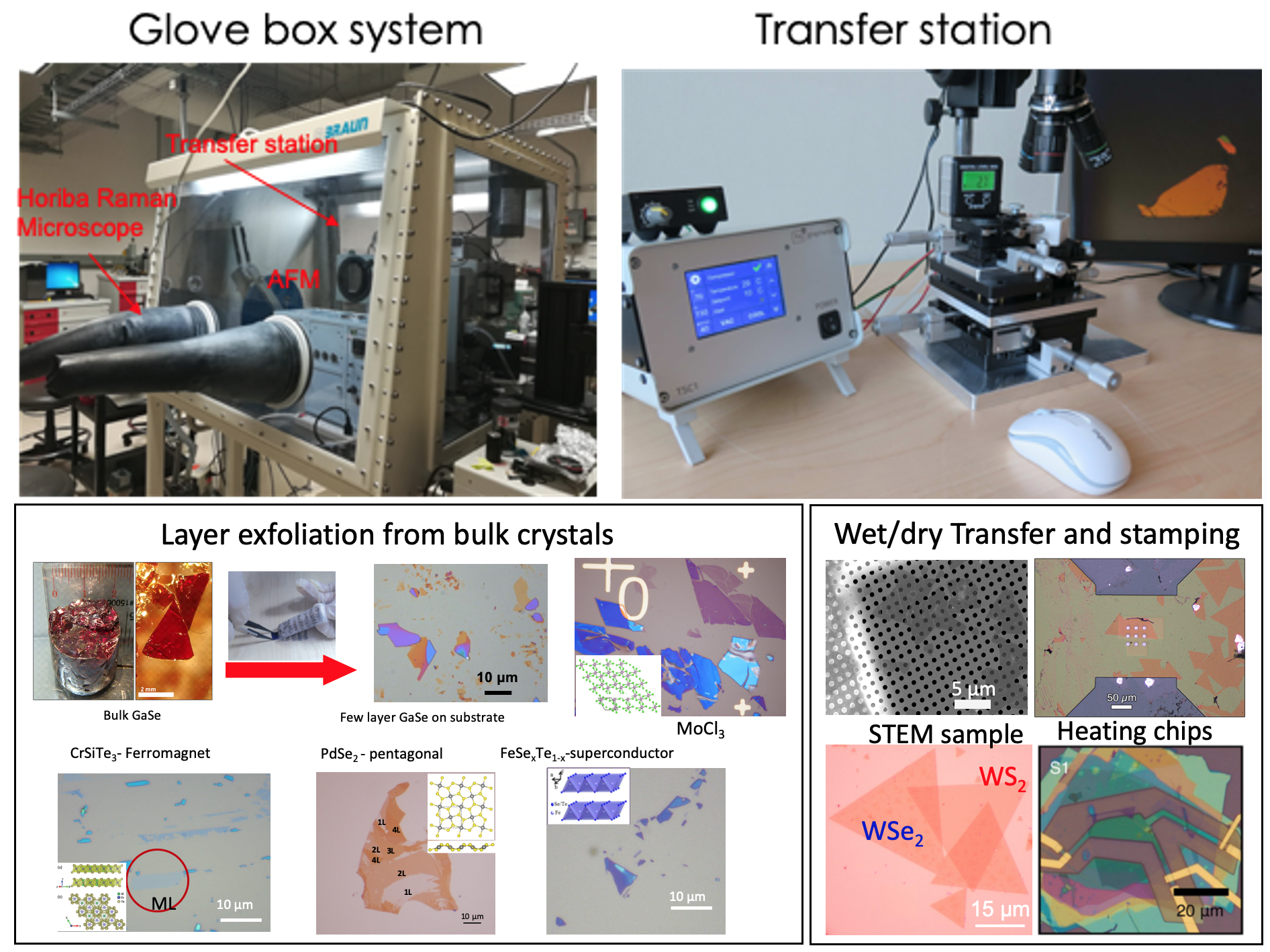
Y. Gu, L. Zhang, H. Cai, L. Liang, C. Liu, A. Hoffman, Y. Yu, A. Houston, A. A. Puretzky, G. Duscher, P. D. Rack, C. M. Rouleau, X. Meng, M. Yoon, D. B. Geohegan, Kai Xiao, Stabilized synthesis of 2D verbeekite: Monoclinic PdSe2 crystals with high mobility and in-plane optical and electrical anisotropy, ACS Nano. 16, 13900 (2022). 

Y. Gu, et al. Two-dimensional PdSe2 with strong in-plane optical anisotropy and high mobility grown by chemical vapor deposition, Adv. Mater. 32(19), 025048 (2020). 

X. Li et al, Isotope-Engineering the Thermal Conductivity of Two-Dimensional MoS2, ACS Nano, 13, 2481(2019).

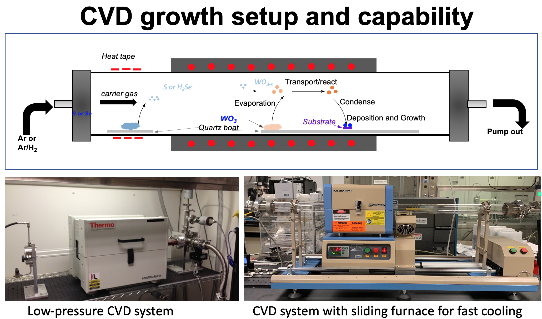
K. Wang, et al., Strain tolerance of two-dimensional crystal growth on curved surfaces, Science Advances 5, eaav4028 (2019).

X Sang, et al., Atomic Insight into Thermolysis‐Driven Growth of 2D MoS2, Advanced Functional Materials 29, 1902149 (2019).

M. Lin, et al., “Ultrathin nanosheets of CrSiTe3: a semiconducting two-dimensional ferromagnetic material”, Journal of Materials Chemistry C, 4, 315 (2016). 

This transfer system allows the exfoliation, deterministic transfer, encapsulation of air-sensitive 2D materials and the construction of numerous heterostructures for 2D electronics and quantum information science.
Chemical vapor deposition (CVD) is a widely used method for the scalable synthesis of most 2D materials.

Advanced synthesis and processing of 2D materials, topological quantum materials, and heterostructures

2D materials display many different atomic and electronic phases offering tremendous opportunities for studying novel quantum topological states, such as QSH, QAH, superconductors, and Weyl/Dirac semimetals etc. We are interested in the synthesis and assembly of 2D quantum materials and heterostructures by both top-down (exfoliation and transfer) and bottom-up (CVD and PLD) approaches. Our goal is to realize novel 2D layered quantum materials and devices by tailoring the heterogeneities including defects, confinement, and symmetry breaking through controlled synthesis and processing for the emerging quantum states (such as quantum emission, QSH, QAH, Majorana fermions).

Subject areas or capabilities: 

—– Synthesis and assembly of 2D quantum materials to create vdW heterostructures which enable to explore the new quantum phenomena from the proximity effect relevant to topological qubits.

—– Synthesis of 2D layered quantum materials such as TMD-based topological materials by CVD, PLD and exfoliation.

—– Assembly of 2D quantum materials to create heterostructure with controlled stacking by the deterministic transfer system which allows transfer and stacking of individual layers in an air-free ‘glove box’.

—– Understand phase formation mechanism during synthesis and develop methods for selective growth and processing of phase-engineered 2D TMDs for 2D electronic and quantum devices. 

—– Quantum device and transport.

K. Xiao, D. B. Geohegan, Laser synthesis and processing of atomically thin 2D materials, Trends in Chemistry, 4, 769(2022) 

A. Oyedele., et al. PdSe2 : pentagonal 2D layers with high Air stability for electronics, J. Am. Chem. Soc., 139, 14090 (2017). 
X. Li, et al, Edge-Controlled Growth and Etching of Two-Dimensional GaSe Monolayers, J. Am. Chem. Soc., 139, 482–491 (2017).

Solution processed flexible polymer and halide perovskite electronics.
Controlled atmosphere glovebox facility for processing air-sensitive, soluble materials including organic, polymer, hybrid materials to make thin film electronic devices such as transistors, photovoltaics, memory devices.

Solution-processing thin film electronics, solar cells, and flexible electronics

HOIPs are fascinating yet mysterious hybrid materials that within a few short years have quickly attained over 25% photovoltaic power efficiency, eclipsing the ~12% efficiencies of organic PV materials. Our research targeted the key scientific questions linking the synthesis, structure, and properties of HOIPs while enhancing and crosscutting many emerging programs across ORNL in hybrid organic/inorganic materials, neutron reflectivity/scattering, chemical imaging, analytic electron microscopy, ultrafast laser spectroscopy, theory modeling, and advanced manufacturing.


J. Chen, S. Das, M. Shao, G. Li, H. Lian, J. Qin, J. F Browning, J. K Keum, D. Uhrig, G. Gu, K. Xiao, Phase segregation mechanisms of small molecule‐polymer blends unraveled by varying polymer chain architecture, SmartMat, 2(3), 367-377 (2021). 

Ran, et al, Electron-beam-related studies of halide perovskites: challenges and opportunities, Advanced Energy Materials, 1903191 (2020).
Yang, Bin, et al. “Real‐Time Observation of Order‐Disorder Transformation of Organic Cations Induced Phase Transition and Anomalous Photoluminescence in Hybrid Perovskites.” Advanced Materials, 30(22) 170580 (2018).
S. Das, et al, “Low Thermal Budget, Photonic-Cured Compact TiO2 Layer for High-Efficiency Perovskite Solar Cells”, J. Mater. Chem. A, 4, 8695 (2016).
B. Yang, et al, “Deciphering Halogen Competition in Organometallic Halide Perovskite Growth”. J. Am. Chem. Soc. 138, 5028 (2016).
S. Das, et al, “Correlating High Power Conversion Efficiency of PTB7:PC71BM Inverted Organic Solar Cells to Nanoscale Structure,” Nanoscale, 7, 1551 (2015).

 
Scroll to Top